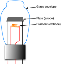
The original tube diode used an evacuated glass tube, a heated
cathode filament, and an anode plate to rectify AC current. They are still
used in high power rectifiers, but fragility, size, and heat creation
(power wasted) have made them all but disappear to specialty applications. Today semiconductors form the basis of
electronics for all the opposite reasons.
Periodic Table Modern electronic devices
are primarily made from semiconductor elements which have as their basis
Silicon (Si) and dopant materials added to silicon such as
Phosphorous (P) and Boron (B) as well as others. Semiconductor action takes advantage of the
quantum properties at the thin boundary layer between to types of doped
silicon P type (positive) and N type (negative) called the junction.
This was discovered at
Bell labs by Dr. Shockley by accident, but the discovery was quickly put to use immediately
outdating tube technology and rapidly becoming increasingly miniaturized
with pressure from the space race and then computer chip technology all of which led to the computer in your pocket.
(the smartphoine was invented in Waterloo Ontario by Blackberry)
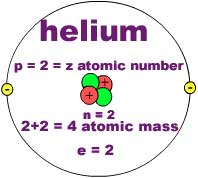
Atoms have a nucleus composed of
positively charged protons and neutral charged neutrons. The # of protons Z (atomic
number defines the atom) is usually equal to the orbiting electrons
which are mass less and have a negative charge. This keeps the atom
neutrally charged.
In
the above example of the simple element helium the atomic
number is 2 ( protons ) and the atomic mass is 4 because
there are also 2 neutrons and the number of electrons is 2 to keep
the charge neutral. The valence shell or orbit of
electrons is 2. The inner or 1st orbital always has 2 and the next
orbitals try to fill with 8 electrons(stable octet)
Remember why conductors conduct?
The
outer valence electrons are loose and free to move when a voltage is
applied.
Semi conductors have outer valence electron that are free to move
under certain conditions thus the term SEMICONDUCTORS
Insulators Conductors
Semiconductors at the Atomic Level
Insulators
- conduct both heat and electrical current POORLY
- organic compounds, gases,
- outer valence electrons are strongly bonded to the nucleus
- at high enough voltage anything will conduct
OXYGEN
Conductors - conduct
heat and electrical current very effectively
- the outer electron(s) in conductive atoms are loosing constrained
by the nucleus and can be moved easily when a voltage is applied
COPPER
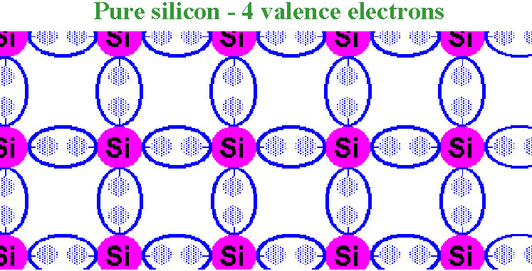
Semiconductors -
mixtures of a primary element such as
Silicone
( or Germanium)
and an impurity (very small amounts) that covalently bonds to
silicone and adds or subtracts a valence electron
- semiconduction phenomena occurs at the
junction between a
P (positive) and an N
(negative) type
doping material
SILICON
MAKING SILICON INTO A
SEMICONDUCTOR
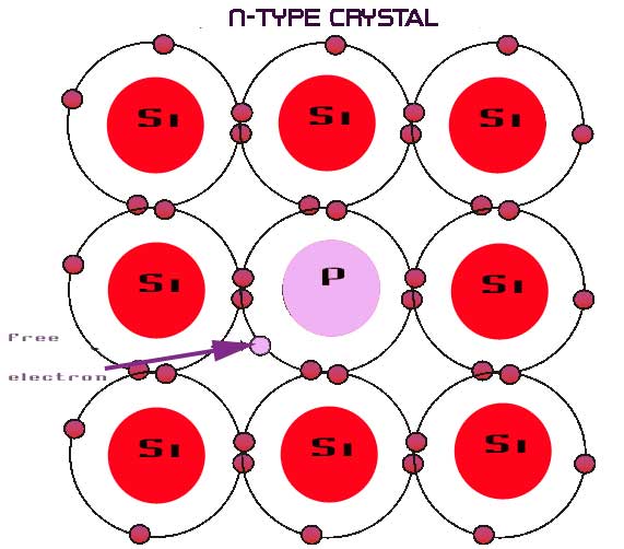
start with silicon then add an
N
or
P
dopant
N (negative) type silicone crystal is made by high temperature diffusion of the dopant impurity Phosphorous a pentavalent atom.
The extra valence electron is free to move under the force of a voltage potential when holes are available.
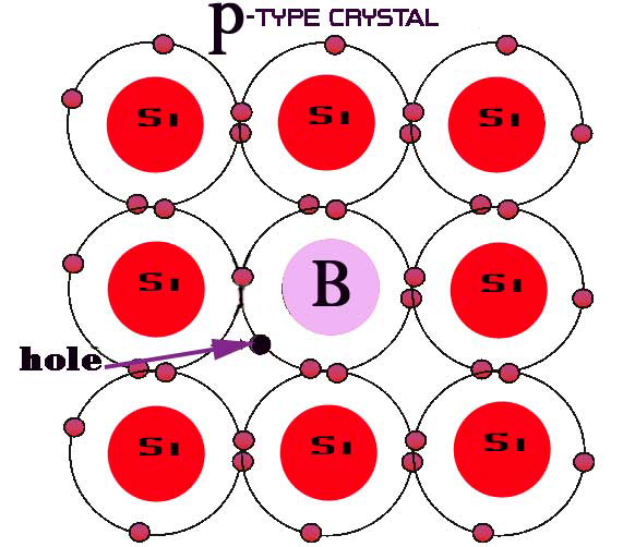
P type crystal is created when the dopant Boron is diffused into
the silicone
crystal lattice
.
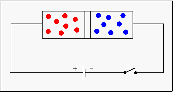
Semiconductor components are made when the N and P type materials are
joined. Interesting things happen at the junction when a forward voltage is applied.
Semiconductor action
1) when the N (phosphorous) and P (boron)are joined at the junction some of the
free electrons from the N side gravitate into the holes on the P side
which creates neutral silicon at the junction called a potential barrier (effectively an insulator).
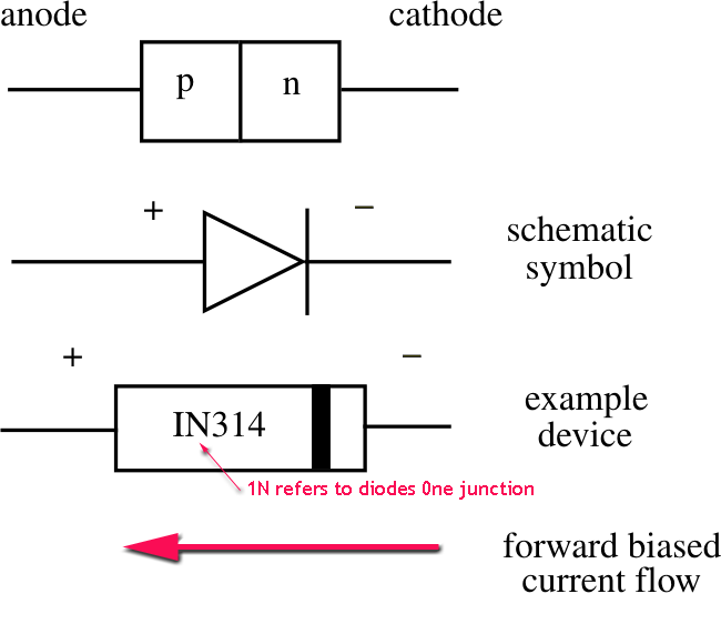
2) if a negative potential is applied at the N side (cathode) the free electrons will repel across the junction and if a positive potential is applied to the P (anode) the positive charge spaces (holes) will move towards the electrons and if a voltage of about .7 volts is applied then current will begin to flow as electrons are pushed towards the holes.
3) this is called forward biasing of the N - P diode junction and .7 volts is now called the forward voltage the energy required to cross the junction.
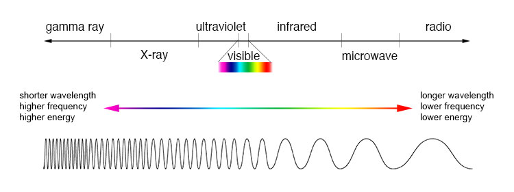
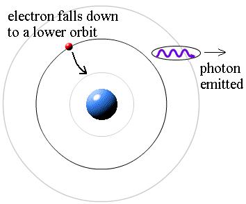
-when electrons cross the junction their energy potential is raised to .7 V . when the electrons drop back to ground state they release a photon of infrared light which is not visible to humans
- LEDs are diodes that have various dopants that raise the forward voltage of the electrons that release photons in the visible range of vision.
For example a forward voltage of 1.8 volts will create photons that appear as Red LED light.
Electromagnetic spectrum colour and energy vs wavelength
4) if the polarity is reversed then free electrons are pulled to the cathode and holes are pulled towards the anode increasing the potential barrier and blocking current flow
5) this is called reverse biasing the junction and almost no current flows
6) the junction can prevent reverse flow of current until the reverse breakdown voltage is exceded and then massive current flows and usually burns out the junction ruining the diode (straw that breaks the camel's back)
7) this is called reverse breakdown voltage , avalanche voltage or Zener voltage

 iode used an evacuated glass tube, a heated
cathode filament, and an anode plate to rectify AC current. They are still
used in high power rectifiers, but fragility, size, and heat creation
(power wasted) have made them all but disappear to specialty applications.
iode used an evacuated glass tube, a heated
cathode filament, and an anode plate to rectify AC current. They are still
used in high power rectifiers, but fragility, size, and heat creation
(power wasted) have made them all but disappear to specialty applications.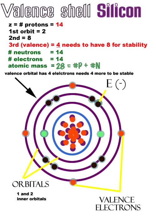
![[Bohr Model of Oxygen]](../images/oxgen.gif)
![[Bohr Model of Copper]](../images/copper.gif)
![[Bohr Model of Silicon]](../images/b0014.gif)